
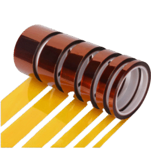
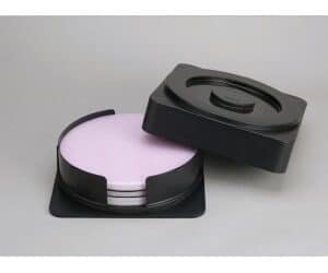
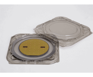
Description
A dicing tape is used for fixing a work piece during the dicing process in the manufacturing of semiconductors, electronic and optical components. With greater diversity and higher quality in chips, dicing tapes also require advanced technology. These dicing tape is used widely in a variety of applications including silicon and GaAs semiconductors (compound semiconductors), encapsulated package substrates, ceramics, glass, and crystals.
Features
- Excellent control to back-side chipping and chip fly-off
- Excellent over-time stability
- Excellent adhesiveness (shape-following properties)
- High performance to EMCs (Epoxy Mold Compounds) and other types of difficult-to-adhere workpieces
- Excellent expandability and smooth peeling
Application
- Silicon (SI), Gallium Arsenide (GaAS) and other type of Semiconductors (Wafers)
- Package substrate (BGA/QFN etc) (Package)
- Glass, crystal
Reviews
There are no reviews yet.